Intro
The Game Boy camera, one one my favourite pieces of hardware so far. I would like to say that I had one since I was a child with some old pictures, but I can’t. I got my Game Boy camera some time around last summer, I even had already started the game boy project, but was thinking more about backing up saves from the regular cartridges.
According to Wikipedia, the Game Boy camera was the smallest digital camera of its time. The resolution of the camera is 128×112 pixels, apparently the sensor can take pictures with double this double this size but they are downscaled in order to be stored in the small RAM memory and shown on the Game Boy screen.
This post is about the process I used to download the pics to the computer, also the problems that came up. It is part of a series here. It may be helpful to read the previous posts, where I explain how the hardware works:
Gameboy Paks to PC interface board.
Game Boy Pak Reader & The Cartridge Header.
Dumping Game Boy MBC1 cartridges.
My board is based on a ATmega32 microcontroller, that sends the data from the cartridge to the PC through a serial link, but the code should be easy to port to any microcontroller of your preference.
Game boy camera Hardware.
While there is a bunch of different types of cartridges for the Game Boy, almost all of them they follow the same structure. The majority of the cartridges have a ROM chip, a memory bank controller and a RAM chip backed up by a battery.
The Game Boy camera is different because it has a controller inside the cartridge responsible for I/O, reading data from the image sensor and putting this data in memory, etc.

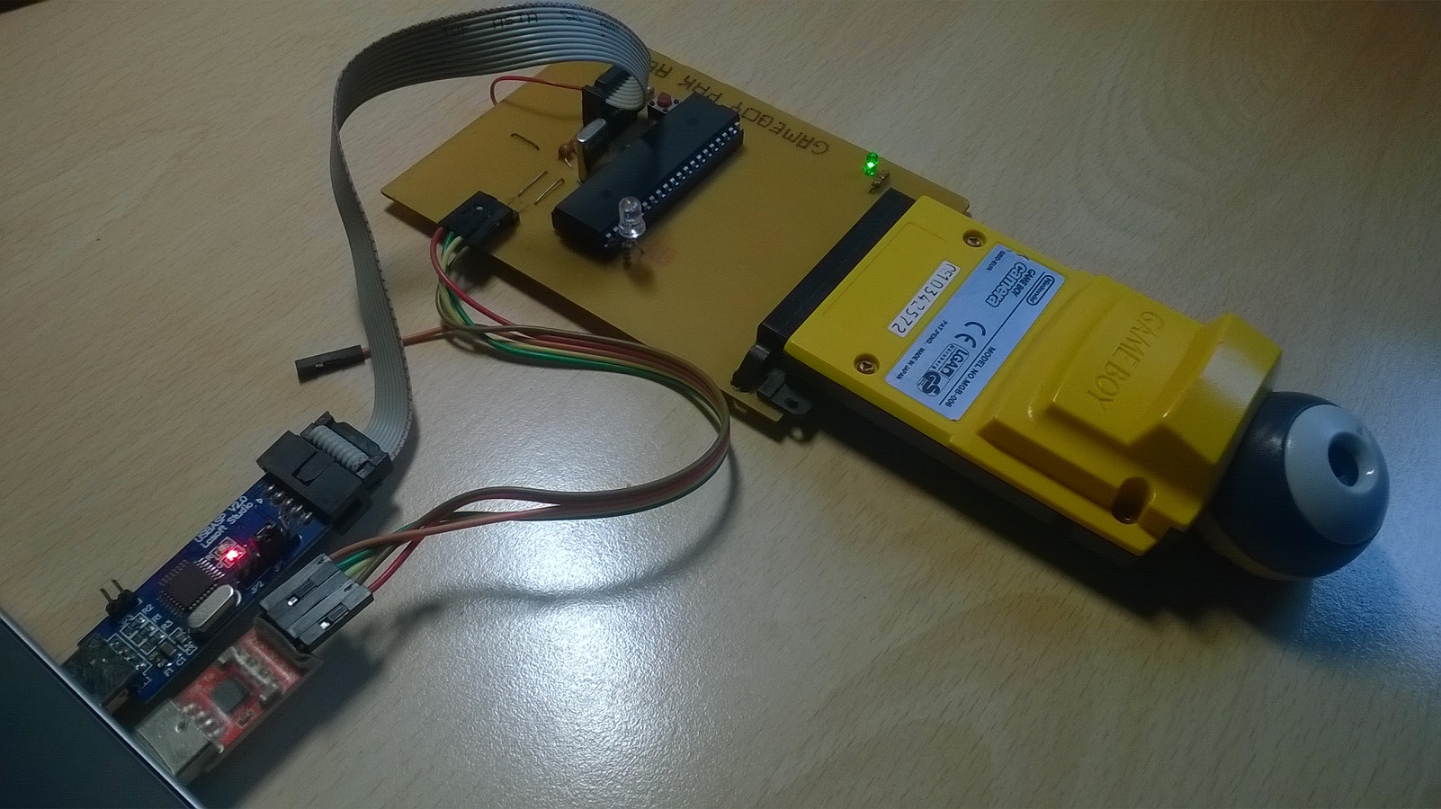
Differently from other cartridges, the memory chips are not accessible through the cartridge connector, all the data must past first through the MAC-GBD chip, seen in the picture above. Below, a picture of the camera connected to my board.
The ROM header
Using the code explained in one my last posts, I read the ROM header and extracted the following information from the cartridge:
Cartridge Connected

Title of the game in ASCII:GAMEBOYCAMERA
Gameboy/Gameboy Color?	Cartridge with no color function

Super Gameboy functions?  Cartridge with SGB functions

Cartridge Type:	Game Boy Camera

ROM size:	8Mbit = 1MByte = 64 banks
RAM size:	1MBit =128kB =16 banks
The MBC5 is the only controller able to manage 128kB of RAM. So I deduced I had to use the same logic used for reading a MBC5 cartridge.
Camera controller.
If the controller inside the camera was similar to a MBC5, it should work as described below. It is simple, for example, if you want to select the RAM bank 5 (0x005), you should write 0x05 in any location from 0x2000 to 0x2FFF and 0x00 in any location from 0x3000 t0 0x3FFF.
0000-3FFF - ROM Bank 00 (Read Only).
4000-7FFF - ROM Bank 00-1FF (Read Only).
A000-BFFF - RAM Bank 00-0F, if any (Read/Write).
0000-1FFF - RAM Enable (Write Only).
0Ah will enable the SRAM, 00h will disable it.
2000-2FFF - Low 8 bits of ROM Bank Number (Write Only).
The lower 8 bits of the ROM bank number.
3000-3FFF - High bit of ROM Bank Number (Write Only).
The 9th bit of the ROM bank number.
4000-5FFF - RAM Bank Number (Write Only).
Writing a value in range for 00h-0Fh maps the corresponding RAM Bank into A000-BFFF.
Be aware that all these locations are from ROM, so when a byte is written, it is ‘ignored’ by the ROM. A byte is written to these locations is captured by the memory controller.
Later, thanks to the great documentation by Antonio Niño Díaz, I discovered that in fact, the controller is similar to a MBC3 described below. The timer register (like in Pokémon cartridge) is ignored.
0000-3FFF - ROM Bank 00 (Read Only)
4000-7FFF - ROM Bank (Read Only)
A000-BFFF - RAM Bank, if any (Read/Write)
0000-1FFF - RAM Enable (Write Only)
0Ah will enable the RAM ,00h will disable it.
2000-3FFF - ROM Bank Number (Write Only)
The ROM Bank Number is written directly to this address.
4000-5FFF - RAM Bank Number
Selects the RAM bank at A000-BFFF.
After creating a code to handle the MBC3 way of doing things, I realised that the differences are only in the ROM part.
The first code I wrote for accessing the Game Boy cartridge is shown below:
ControlPort&=~(1<<MREQ);//Memory Requirement, Enables the RAM chip
if (MBC==3){
	//WriteByte(0x1000, 0x0A);//enable RAM
	for (uint8_t i=0;i<0x0F;i++){
		WriteByte(0x5000,i);//select bank
		for (uint16_t j=0xA000;j<=0xBFFF;j++){//Read the RAM bank
			uart_putc(readByte(j));
		}
	}
	//WriteByte(0x1000,0x00);//disable RAM
}
ControlPort|=(1<<MREQ);
Most of the documents about the MBCs say that the RAM should be enabled by writing a 0x0A to 0x0000-0x1FFF area before reading or writing. I always use that with cartridges, but according to Antonio’s documentation about the camera, the should be enabled just for writing.
A python script on the computer side receives the data and put it into a file.
ramsize=128*1024 #128KB
numBytes=0
        name=input("What is the name of the file?")
        f = open(name, 'ab')
        timeout=20
        while (numBytes<ramsize and timeout>0):
            timeout=20
            while ser.inWaiting()==0:
                print("waiting...\n",numBytes)
                time.sleep(0.1)
                timeout=timeout-1
                print("timeout:",timeout)
                if(timeout==0):
                    break
            data = ser.read(1)#must read the bytes and put in a file
            f.write(data)
            numBytes=numBytes+1
        f.close()
With that code I got the following result:

Not a good result at first, but scrolling a bit more:
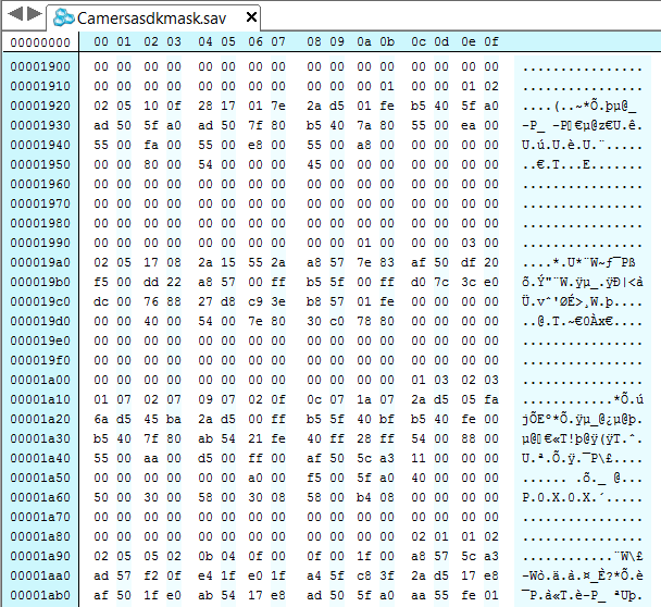
Awesome! Randomness is expected in a experiment like this. However, the first 8kB seemed to repeat thorough the file.
I used the executable version of tool called GBcameraDump, by Bob Baffy, to convert the save into bitmaps. I really would like to study how the images are compressed, but now I wanted to focus on transferring the save to the PC. The source code for GBcameraDump is available here.
Later, I could check that this is the first bank (sort of expected). According to the file here, the first bank is a working memory and the pictures are stored from the second bank onwards. For some reason, I could not in any way change the RAM banks. I wrote some code for changing ROM banks and could see that it worked, only the RAM was the problem.
This happened maybe some weeks ago, as I have college stuff to do I usually put my projects away for some time. This way I also can refresh my mind and have new ideas to experiment.
Some weeks later
Perhaps I was not using the right locations? If there was a mistake in the documentation? Sometimes a bit in the wrong place is sufficient to mess up a whole project. I decided that would not hurt disassemble the ROM that could read from the camera to see the exact values the camera uses to change banks. The disassemble tool that I used was written by Maciej Muszkowski and is available here.
The beginning of the ROM disassembled:
[0x00000100] 0x00           NOP
[0x00000101] 0xC3 0x50 0x01 JP $0150
[0x00000150] 0x31 0xFE 0xFF LD SP,$FFFE
[0x00000153] 0xF3           DI
[0x00000154] 0xAF           XOR A
[0x00000155] 0xE0 0x0F      LDH [$0F],A
[0x00000157] 0xF0 0x40      LDH A,[$40]
[0x00000159] 0xCB 0x7F      BIT 7,A
[0x0000015B] 0x20 0x04      JR NZ,$04 ; 0x161
[0x0000015D] 0xCB 0xFF      SET 7,A
[0x0000015F] 0xE0 0x40      LDH [$40],A
[0x00000161] 0x01 0x02 0x00 LD BC,$0002
[0x00000164] 0xCD 0x7D 0x09 CALL $097D
[0x00000167] 0xF0 0x44      LDH A,[$44]
[0x00000169] 0xFE 0x91      CP $91
[0x0000016B] 0x38 0xFA      JR C,$FA ; 0x167
[0x0000016D] 0x3E 0x80      LD A,$80
[0x0000016F] 0xE0 0x40      LDH [$40],A
[0x00000171] 0xAF           XOR A
[0x00000172] 0xE0 0x47      LDH [$47],A
[0x00000174] 0xE0 0x48      LDH [$48],A
[0x00000176] 0xE0 0x49      LDH [$49],A
Ok, the tool for disassembling worked pretty well. Now, I needed to see which instruction writes a byte to memory. From the Game Boy Programming Manual:

Great! I looked for this instruction and found the following code(the code after ‘;’ represents a comment):
[0x0000018A] 0x3E 0x00      LD A,$00
[0x0000018C] 0xEA 0x00 0x00 LD [$0000],A ;write 0x00 to the Enable RAM location
[0x0000018F] 0x3E 0x01      LD A,$01
[0x00000191] 0xEA 0x00 0x20 LD [$2000],A ;selects ROM bank 1
[0x00000194] 0x3E 0x00      LD A,$00
[0x00000196] 0xEA 0x00 0x40 LD [$4000],A ;selects RAM bank 0
If the manual asks to write a byte to area 0x0000-0x1FFF, I think that I should use a location in the middle, like 0x1000. It is not logical, just the way I though it should be better. Ends up that always the beginning of each area is used by the camera code.
The code above must be some sort of initialisation code as it sets the first ROM and RAM banks, and also disables the RAM.
With the new values, the code for reading the RAM was like the following:
ControlPort&=~(1<<MREQ);
if (MBC==3){
	for (uint8_t i=0;i<0x0F;i++){
		WriteByte(0x4000,i);//select bank
		for (uint16_t j=0xA000;j<=0xBFFF;j++){//Read the RAM bank
			uart_putc(readByte(j));
		}
	}
}
ControlPort|=(1<<MREQ);
Guess what? I did not work! I got the same thing, the first bank over and over again, and I was stressed. But it was not expected to work anyway, if the engineers give a whole area to developers use, it should work in any location.
The last attempt
I played some games, went out, and made fun of the Zelda CDi games with friends. Still, I knew that I would not rest before getting these pictures on the computer.
Since the beginning, I knew that I could hook up wires to the camera and check the data with a logic analyser. In fact it would make the work easier. But I surely would not under any circumstance solder anything to my GB camera. Also, the SMD components make it impossible to use grabbers.
Also, I knew that the Game Boy camera uses the PHI signal. The Game Boy feeds a clock signal around 1MHz to the cartridge slot, but almost none cartridge uses it. The camera documentation by Antonio Díaz says that the clock signal is not necessary for reading data from RAM or changing banks. In addition, I confirmed that I could read the ROM with no problems without driving the PHI pin.
Anyway, I searched the manual for something about the PHI signal in the Game Boy Manual.

For some luck, I fell in this page from the manual. The manual refers to the PHI signal as CLK, by the way I don’t know what PHI stands for. Feel free to comment ^^.
The CS(MREQ, memory requirement) line represented in the diagram above is used to disable the ROM and enable the RAM chip. Before, with regular cartridges, I used to change RAM banks without pulling the MREQ line high and it always worked. Maybe I should have to pull the MREQ high before changing bank, it seemed reasonable.
Then, code with the necessary modifications was:
if (MBC==3){
	for (uint8_t i=0;i<0x0F;i++){
		WriteByte(0x4000,i);//select bank
		ControlPort&=~(1<<MREQ);//inside the loop now.
		for (uint16_t j=0xA000;j<=0xBFFF;j++){
			uart_putc(readByte(j));
		}
		ControlPort|=(1<<MREQ);
	}
}
I just made the MREQ signal be changed only when RAM is accessed.
Let’s see the file I download with the code above:
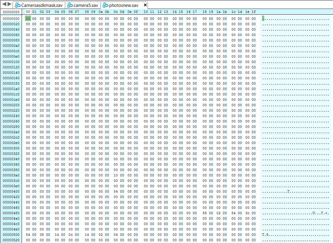
Unusual, but id it work?
Yes! I used GBcameraDump to check the file and jackpot!

Some of the photos:
That is it. It was hard to get these pictures, but I think it totally worth it. The project of the Game Boy board is still incomplete, but I feel that I learn something important every step I take. You can download the files for the project here. Sorry, I still have not stopped and tried to learn how to use github, but it is in my list :)
Thanks for reading! Comment if you have any question.
Time to go around and take lots of 8 bit pictures! See ya next post. o/
Sources
Game Boy Camera RE – by Antonio Niño Díaz, Github:
https://github.com/AntonioND/gbcam-rev-engineer
gb-disasm – A game boy disassembler by Maciej Muszkowski. Github:
https://github.com/mmuszkow/gb-disasm
GBcameraDump – by Bob Baffy, I used a executable, but the source is available at:
https://github.com/unnamedculprit/GBCameraDump
Memory Bank controllers – Gameboy Development Wiki.
http://gbdev.gg8.se/wiki/articles/Memory_Bank_Controllers
Gameboy CPU manual:
http://marc.rawer.de/Gameboy/Docs/GBCPUman.pdf
Gameboy camera RAM format:
http://www.devrs.com/gb/files/gbcam.txt







Muito bacana, parabéns pelo ótimo trabalho e por documentar a sua jornada!
Muito obrigado!
This is really cool. I feel like you could make some money taking peoples gameboy cameras, and giving them the photos on them. Might be interesting. Sorry that this isn’t Portuguese. No hablo.
Don’t worry, I am fine with English.
Hahaha. Nice idea!
Hi,
MREQ stands for “memory request”. As distinguished from “IORQ”, IO request. On the original Z80 CPU these were separate, since the Z80 has 2 uses for the address bus, one for RAM, one for I/O. The difference being, the IN / OUT instructions assert the IORQ pin, other instructions assert the MREQ pin.
The IN / OUT Z80 instructions were removed from the Gameboy’s CPU, as well as some other Z80 ones. But I suppose the MREQ pin stayed. Of course the Z80 also had built-in RAM refresh logic, so I suppose it was important to make sure only RAM was responding to requests when MREQ was asserted. Since the Z80 would send out requests for RAM it wasn’t using, just to keep it refreshed. You wouldn’t want those refresh cycles to trigger any other hardware you had on the bus.
CPUs like the 6502 didn’t have RAM refresh, so IO was memory-mapped. But that made IO decoding a bit more complex, and you had to implement refresh hardware yourself. Bleh!
A guess on PHI… some old cpus (6502, bleh!) used a 2-phase clock. 2 clock pins, with particular requirements for their timing. So PHI could be “phase 1”. Of course there is no PH2, because the Z80 only needed 1 clock phase (hooray!).
So why even mention clock phases? At the time, Nintendo used the 6502 in the NES. So their hardware guys would have a lot of experience with that, and maybe, particularly with the likelihood of lots of the design being done in Japanese and translated later, PHI stuck around as a name for the clock line.
Possibly!
Nice site anyway, very good work!
Sam xxx.
Hello Sam.
Thanks for your very informative comment!
You really know you microprocessor stuff. Do you work with emulators or something?
Thanks again.
Robson